Rapidus 2nm Pilot Lands Canon, 60 Customers in Talks
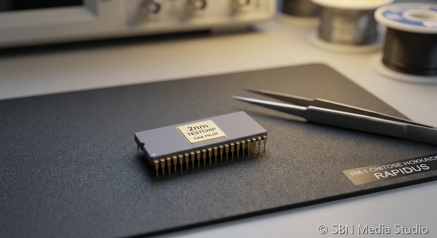
MAY 27, 2026 — CHITOSE, HOKKAIDO, JAPAN. Japan's Rapidus has moved its IIM-1 fab from construction phase into active 2nm gate-all-around pilot-wafer production and confirmed Canon as its first paying customer, with the inaugural chip designed on Synopsys EDA tooling, according to Electronics Weekly. CEO Atsuyoshi Koike disclosed that more than 60 additional firms — most based outside Japan and concentrated in high-performance computing, AI accelerators, and edge inference — are in commercial discussions, with 10 already in receipt of preliminary price quotes.
The funding picture has stabilized in parallel. Rapidus secured ¥167.6 billion in private investment earlier this quarter, taking total committed capital across government grants and private equity to roughly $1.7 billion, per Tom's Hardware. That capital base — backed by Toyota, SoftBank, Sony, and METI — is what kept the 2027 mass-production target on the public roadmap after persistent skepticism that a greenfield 2nm fab could match TSMC, Samsung, or Intel on cycle time. The Chitose pilot line is running IBM-licensed nanosheet transistor architecture, which TrendForce notes is the same GAA family Samsung is using at 2nm, putting Rapidus on a fundamentally compatible IP track rather than a divergent one. DigiTimes reports that the packaging-line build at the same Chitose campus is scheduled to align with the front-end ramp, giving Rapidus a co-located back-end capability that few greenfield foundries have attempted at this scale.
The Canon customer disclosure matters because it answers the single open question on Rapidus's commercial viability: whether a Japanese leading-edge foundry could win paid tape-outs at all. Canon is a strategic fit — its lithography arm Canon Tokki and the parent group share equipment and patterning interests with Rapidus — but it is still a transactional customer relationship rather than a captive one. TechSpot reports the April 2026 start of an advanced packaging pilot at the Chitose campus extends the offering beyond front-end fab service, putting Rapidus closer to a full TSMC-style package-and-test stack and giving the 60-customer pipeline a more credible commercial proposition heading into Computex week.
The 60-firm pipeline composition is also notable. Koike's disclosure that most prospective customers are based outside Japan signals Rapidus is being positioned as a geopolitical second source rather than a domestic-substitution play. That framing matters to US AI start-ups and European industrial customers who have struggled to secure leading-edge wafer allocation against the Nvidia, AMD, and Apple commitments that dominate TSMC's 2nm book. Tom's Hardware estimates Rapidus's 2027 volume target sits in the low tens of thousands of wafer-starts per month — a small slice of global advanced capacity, but enough to host a meaningful AI-accelerator or HPC tape-out program for customers shut out elsewhere.
The IBM-licensed nanosheet IP track gives Rapidus an unusual advantage in design-tool readiness. Synopsys and Cadence have already qualified PDKs against the same transistor family for Samsung's 2nm SF2 node, which compresses Rapidus's customer onboarding timeline relative to a from-scratch process. Tom's Hardware notes the company is also leveraging single-wafer processing throughout the IIM-1 line — a higher-cost-per-wafer methodology that trades unit economics for faster cycle time, betting that early customers will pay a premium for tape-out turnaround rather than per-wafer cost parity with TSMC. That bet only works if yield converges quickly: the 10 quoted customers will be watching defect-density data from the pilot wafers over the next two quarters before committing to firm orders.
Rapidus is no longer a policy bet — it is now a functioning 2nm pilot foundry with a paying customer, a real pipeline, and a packaging side. The execution risk between today and 2027 ramp remains substantial, particularly on defect-density convergence and on hiring an experienced cleanroom workforce in Hokkaido, but the conversation has shifted from whether Japan can host a fourth leading-edge foundry to whether Rapidus can clear yield gates fast enough to absorb the AI-side demand that TSMC and Samsung cannot.
Sources
Tom's Hardware, TrendForce, Electronics Weekly, TechSpot, DigiTimes