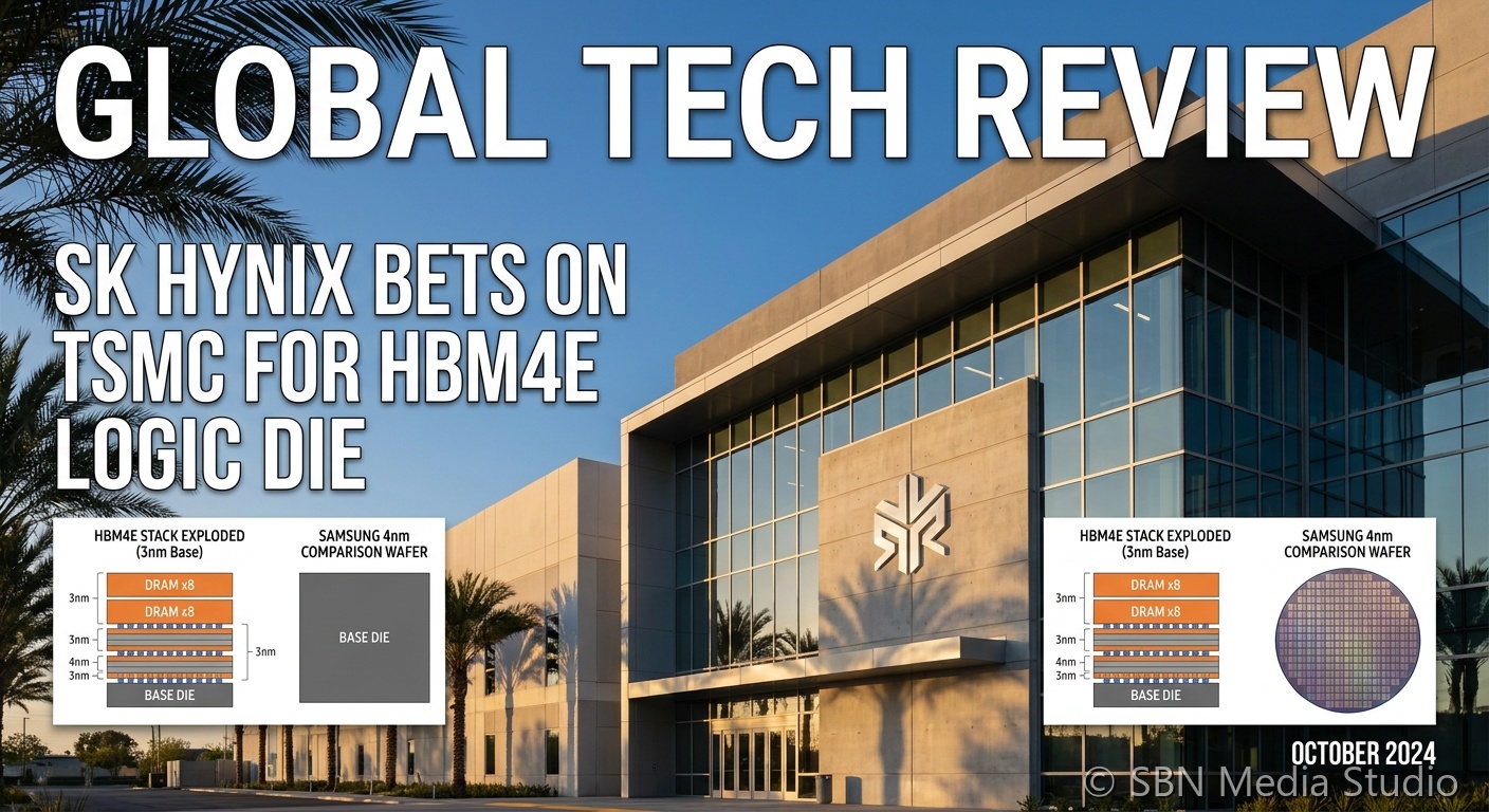
SK Hynix Bets TSMC 3nm for HBM4E Logic Die
SEOUL, JUNE 1, 2026. SK Hynix is moving the logic-die portion of its next-generation HBM4E stack to TSMC's 3nm node, deepening the memory-logic integration story the Korean memory leader showcased at TSMC's 2026 North America Technology Symposium and opening a clear architectural gap with Samsung.
The decision, first reported by TrendForce and corroborated by DIGITIMES, hardens what had been a hedged sourcing posture. SK Hynix had previously qualified both its in-house process and a TSMC 3nm flow for the base-die that sits underneath the HBM4E DRAM stack and handles I/O, ECC, and increasingly custom compute. Choosing TSMC 3nm for production puts SK Hynix on the same logic node as the NVIDIA, AMD, and Broadcom accelerators its HBM stacks plug into — a co-design pitch that has resonated with hyperscalers asking for HBM4E with custom controllers and on-die accelerators. Samsung, by contrast, is staying with its in-house 4nm for HBM4E base-die, betting that captive capacity will let it undercut on price even at a node disadvantage.
The mechanism is straightforward and unforgiving. On HBM4 generations the base-die is no longer a passive plumbing layer: it is a customer-specific logic chip that integrates buffer, test, repair, and increasingly small inference accelerators. Putting that die on TSMC 3nm gives SK Hynix roughly 30% better power-performance and the ability to integrate higher-density SRAM and faster SerDes than a 4nm flow allows. The trade-off is wafer cost — TSMC 3nm wafers run roughly $20,000 apiece versus around $13,000 for a comparable 4nm wafer — which SK Hynix is willing to absorb because the base-die is a tiny fraction of total HBM4E stack BOM and customer pricing power is firmly with the memory supplier right now.
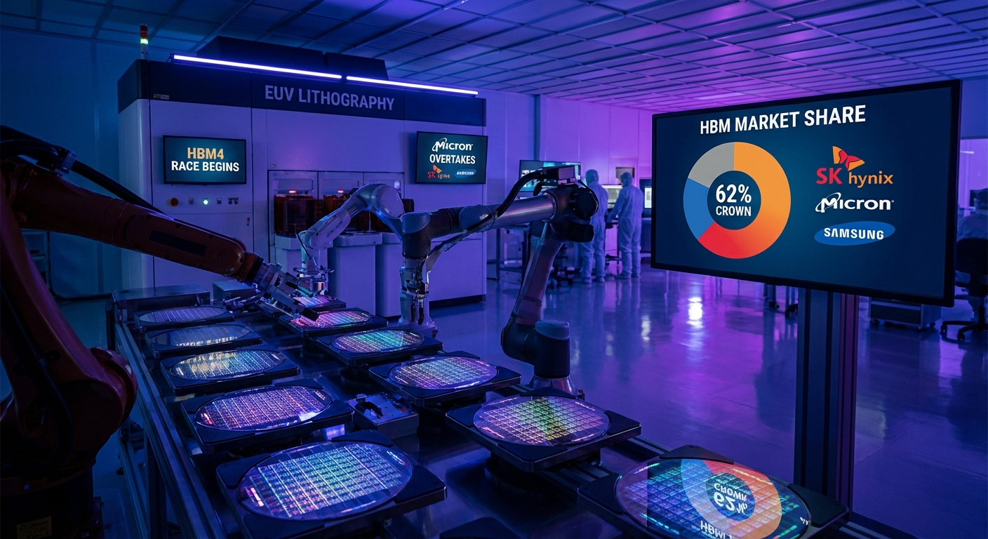
The consequences land on three fronts. First, the timing: DIGITIMES notes HBM4E custom designs across SK Hynix, Samsung, and Micron are due to wrap up in May or June 2026, with NVIDIA already opening orders for 16-Hi HBM4 stacks at the three vendors, per TweakTown. SK Hynix is moving to lock the highest-margin slots first. Second, market share: SK Hynix already holds roughly 50% to 62% of the HBM market by revenue, and a TSMC-fabbed base-die is the kind of differentiation that defends that lead into the HBM4E ramp in late 2027. Third, capex: the company has raised its 2026 infrastructure investment to more than 4x the prior plan, much of it tied to M15X in Cheongju and a new fab in Yongin's semiconductor cluster, signalling confidence that the demand curve justifies the bet.
The takeaway is that the HBM race is no longer just about stacking more DRAM dies — it is about who controls the logic underneath. By outsourcing the base-die to TSMC 3nm, SK Hynix is conceding wafer margin in exchange for a co-design advantage with the AI accelerator vendors that buy almost all of its HBM output. Samsung will have to either match the move, win on price, or accept a structural performance gap heading into 2027.
Sources
TrendForce, DIGITIMES, TweakTown