The Tech Room
Weekly semiconductor intelligence — foundries, memory, equipment, packaging, geopolitics
Read LatestFeatured Story

Huawei Ascend 950PR + 'Tau Scaling Law' Challenge NVIDIA
Huawei's Ascend 950PR hits 1.56 PFLOPs at ~2.8x H20 FP4 throughput on SMIC N+2, paired with a new Tau Scaling Law architecture targeting $12B AI-chip revenue in 2026.
Read Full Analysis →Semiconductors
Huawei Ascend 950PR + 'Tau Scaling Law' Challenge NVIDIA
Huawei's Ascend 950PR hits 1.56 PFLOPs at ~2.8x H20 FP4 throughput on SMIC N+2, paired with a new Tau Scaling Law architecture targeting $12B AI-chip revenue in 2026.
NVIDIA Plants Flag in Taipei: Constellation HQ + CoWoS Lock
NVIDIA pre-commits >50% of TSMC CoWoS capacity through 2027 for Vera Rubin and unveils Constellation, a 50-year-lease Taipei HQ targeted for full ops by 2030.
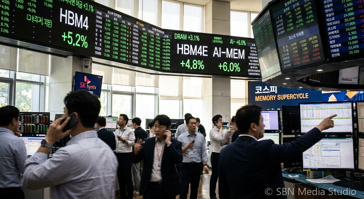
SK Hynix Bets TSMC 3nm for HBM4E Logic Die
SK Hynix is moving HBM4E base-die fabrication to TSMC 3nm, widening the gap with Samsung's 4nm just as NVIDIA opens 16-Hi HBM4 orders and SK Hynix holds ~62% share.
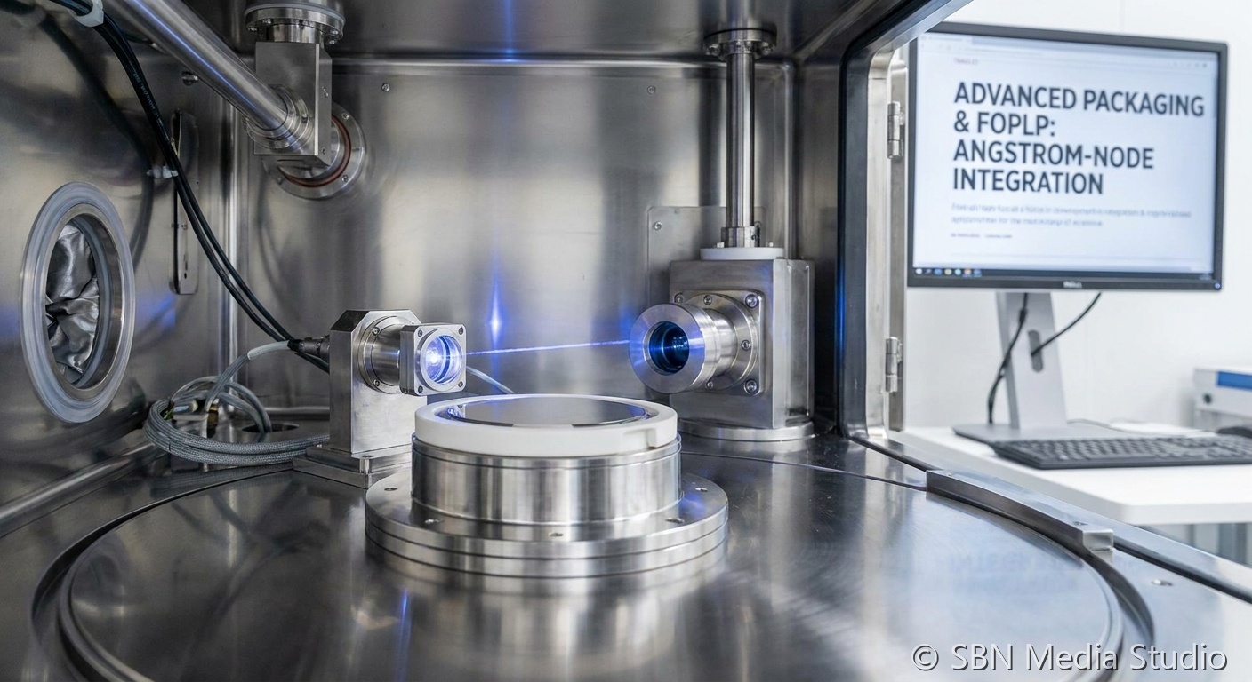
AMD Zen 7 Targets TSMC A14 With Powertech FOPLP Packaging
AMD Zen 7 'Grimlock' CCDs are slated for TSMC 1.4nm A14 with Powertech FOPLP packaging under evaluation, signaling the first credible break from CoWoS for 2028.
Rapidus 2nm Pilot Lands Canon, 60 Customers in Talks
Japan's Rapidus has begun 2nm gate-all-around pilot wafers at IIM-1 with Canon as first paying customer and 60+ firms in commercial discussions ahead of 2027 ramp.
SK Hynix Becomes Asia's 3rd-Largest Co. on HBM Supercycle
SK Hynix shares up 186% YTD at 1,680,000 won as Microsoft, Google, and Amazon offer to bankroll HBM capacity expansion. Q1 operating margin of 72% tops Nvidia.
ASML Says First High-NA EUV Chips Arrive in Months as Intel and SK Hynix Lead Adoption
ASML chief executive Christophe Fouquet told the imec Future Summit in Antwerp on May 19, 2026 that the first commercial chips produced on the company's next-ge
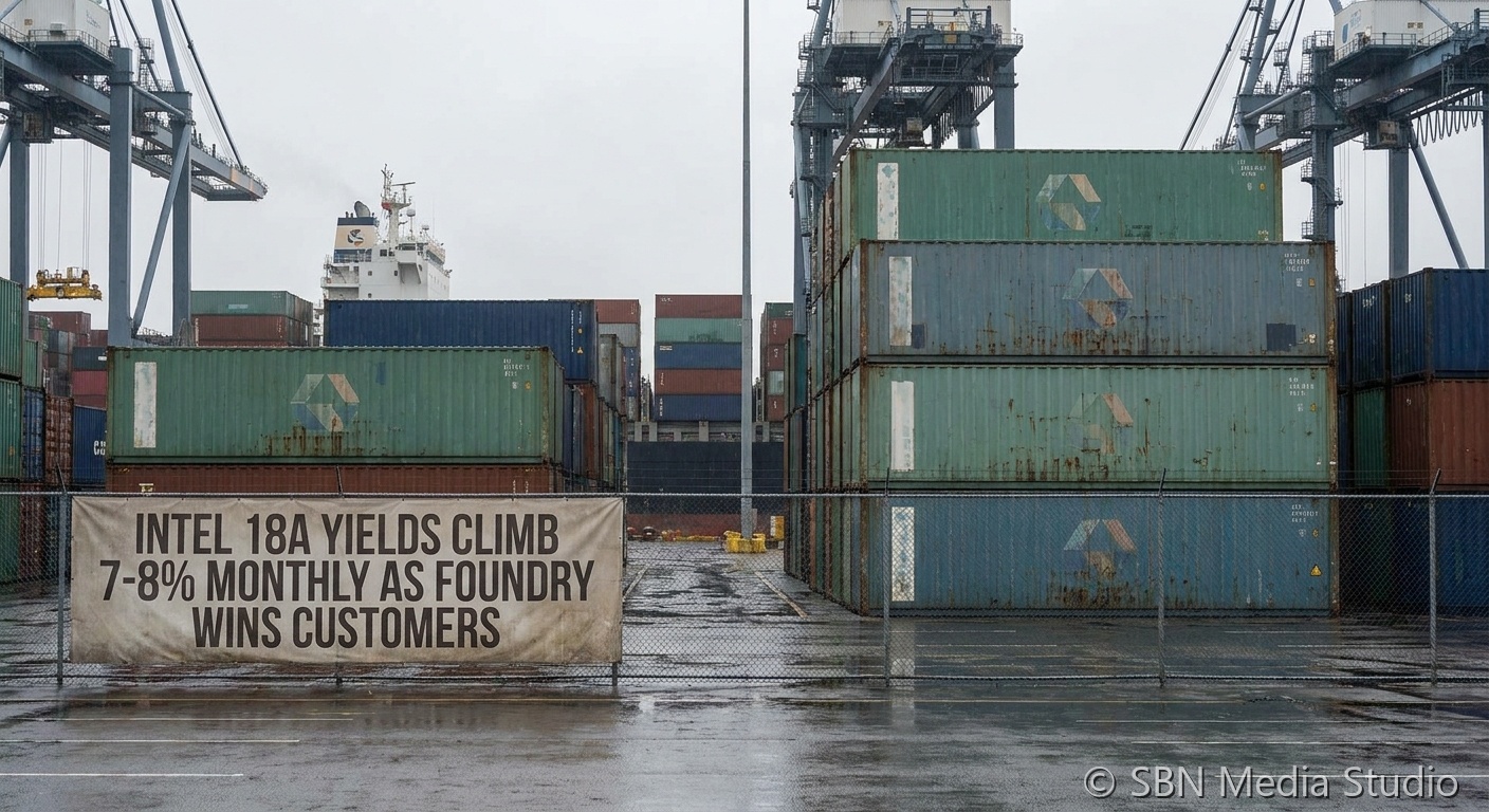
Intel 18A Yields Climb 7-8% Monthly as Foundry Books Multiple New Customers
Intel chief executive Lip-Bu Tan told CNBC on Monday, May 18, 2026 that the company's foundry turnaround is now visible in the numbers, with 18A process yields
TSMC CoWoS Yields Reach 98% as AI Packaging Capacity Doubles in 2026
TSMC told customers at the Hsinchu session of its 2026 Technology Symposium on May 14, 2026 that CoWoS advanced-packaging yields are now above 98% across its vo
Week 13 — March 2026
Micron's record quarter, Samsung's 2nm comeback, NVIDIA capacity reallocation
Never miss a breakthrough.
The biggest moves in the semiconductor industry — delivered straight to your inbox. Trusted by industry professionals.
Free forever. Unsubscribe anytime. Or go Premium for $5/mo →